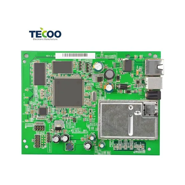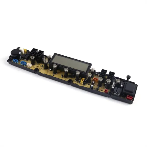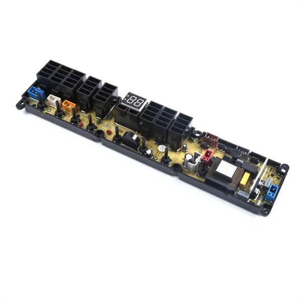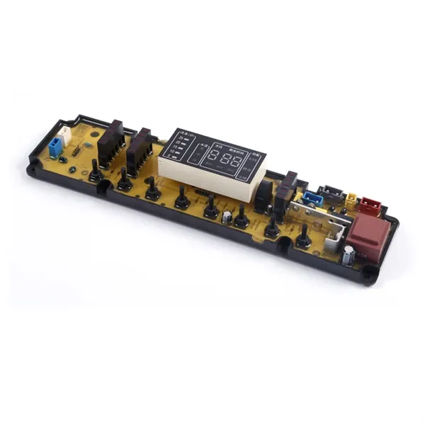

How DFM (Design for Manufacturing) Improves Your PCB Project
In electronics manufacturing, decisions made during the PCB design phase directly impact product yield, production costs, and time-to-market. Statistics show that 70% of manufacturing defects stem from oversights during the design phase (Source: IPC-2022 Industry Report). Design for Manufacturing (DFM) can significantly reduce risk and enhance competitiveness by optimizing the synergy between design specifications and manufacturing processes. This article will delve into DFM's core principles, implementation strategies, and real-world cases, providing engineers with practical optimization solutions.
PCB design often focuses on functional implementation, while manufacturing must contend with process constraints (such as minimum line width and aperture accuracy) and cost pressures. For example, a medical device manufacturer failed to consider the proper alignment of BGA pads with stencils, resulting in 30% solder joint failures. The core goal of DFM is to anticipate and resolve these conflicts during the design phase.
Cost Control: Optimizing material utilization (such as panelization) can reduce board waste by 15%-30%.
Yield Improvement: Through standardized pad design, one manufacturer reduced soldering defect rates from 8% to 1.5%.
Lead Time Reduction: Anticipating manufacturing bottlenecks can shorten pilot production cycles by 40%.
Sustainability: Using halogen-free materials and low-power designs complies with RoHS/REACH standards.
Thermal Management Optimization
High-power components (such as CPUs and MOSFETs) should be placed away from heat-sensitive areas, and heat dissipation vias or metal substrates should be designed. For example, an industrial controller reduced junction temperature by 22°C by increasing the copper foil area.
Signal Integrity Assurance
High-speed signal layers utilize a four-layer board structure, with critical signal lines protected by ground planes. Tools such as SIwave are used to verify impedance matching and prevent signal reflections. Modular Partitioning
Physically isolate power, analog, and digital circuits, and reduce crosstalk through shielded vias.
Pad Size Rules
Recommended window size for 0.4mm pitch QFP pads: Pad diameter = pin pitch × 1.5 (0.4mm pitch corresponds to a 0.6mm pad). A pad that is too small can easily lead to insufficient solder paste, while a pad that is too large can cause shorts.
Stencil Design Collaboration
Step stencils are used to address uneven solder paste flow for 0201 packages. Using this solution, one SMT production line has improved placement accuracy to ±15μm.
Substrate Property Matching
Rogers 4350B (Dk=3.66@1GHz) is used for high-frequency applications, while FR4 (Dk=4.5) is used for conventional digital boards. The compatibility of the material's CTE (coefficient of thermal expansion) and the copper foil's roughness needs to be verified.
Etching Compensation Factor
Set a line width compensation value of 10%-15% to offset undercutting during the etching process.
Reflow Profile Optimization
Use a Ramp-Soak-Spike (RSS) curve to control the peak temperature within 245°C ± 5°C to prevent IC damage.
Test Point Layout Specifications
Set a test point for every 10 cm² of the power network, and maintain a 3-mil safety distance from the edge of the via.
Design for Testability (DFT)
Adding a boundary scan chain and JTAG interface reduces fault location time by 70%.
BOM Management
Specify component tolerances (e.g., ±1% for resistors), lot numbers, and alternatives. Cross-departmental collaboration mechanism
Establish joint design-process review meetings and use 3D models for pre-assembly verification (recommended tool: Siemens NX).
Tool Type Recommended Tool Core Function
DFM Check Valor NPI Real-time Rule Checking and Process Simulation
Signal Integrity HyperLynx Impedance Analysis and Crosstalk Prediction
Thermal Simulation Altium Designer Thermal Distribution Visualization
Collaboration Platform Siemens Teamcenter Version Management and Cross-Departmental Collaboration
1. Concept Phase: Define DFM goals (e.g., yield ≥98%) and collect manufacturability data.
2. Design Phase: Apply constraint-driven design and embed a manufacturing rule library.
3. Verification Phase: Simulate the production process through virtual manufacturing.
4. Production Phase: Continuously collect SPC data and iteratively optimize design rules.
Case 1: DFM Refactoring for 5G Base Station PCBs
Problem: A manufacturer's 28-layer backplane experienced excessive signal attenuation due to inter-layer alignment errors.
Solution:
·Using LDI laser direct writing technology, line width tolerance was controlled to ±0.02mm.
·Introducing buried and blind vias, reducing the number of through-holes by 30%.
Result: Signal integrity improved by 40%, and BOM cost reduced by 18%.
Case 2: Breakthrough in Miniaturization of Wearable Device PCBs
Challenge: Solder reliability of 0.2mm pitch BGA packages.
Innovation:
·Using the Via-in-Pad process to fill the bottom pad.
·Using a trapezoidal design for the stencil openings (0.12mm top, 0.08mm bottom).
Result: Void rate reduced from 15% to 3%, passing MIL-STD-883 vibration testing.
Generate PCB layout solutions that meet multiple constraints using a GAN network, for example:
· Input: Power consumption <5W, signal integrity >60dB, cost <$200
·Output: Optimal stackup and component placement.
5.2 Digital Twins and Real-Time Error Correction
Deploy digital twin systems on production lines to map production data in real time and provide feedback to the design side. In one case, this technology reduced defect detection time from 24 hours to 15 minutes.